Background
Components of micro- and nanoelectromechanical systems (MEMS and NEMS) may be subjected to sustained, shock, or repeated loading or a combination of all three. For system reliability the parts must not fail during normal operation. Consider a resonator found in a cell phone; it must operate at MHz-GHz frequencies for years at a time. This means the fatigue life of the resonator must be greater than 1014 cycles! Strength behavior at nm to micron length scales can be quite different than for bulk materials. The high surface to volume ratio causes strength properties to be highly dependent on the mechanical and chemical surface properties.
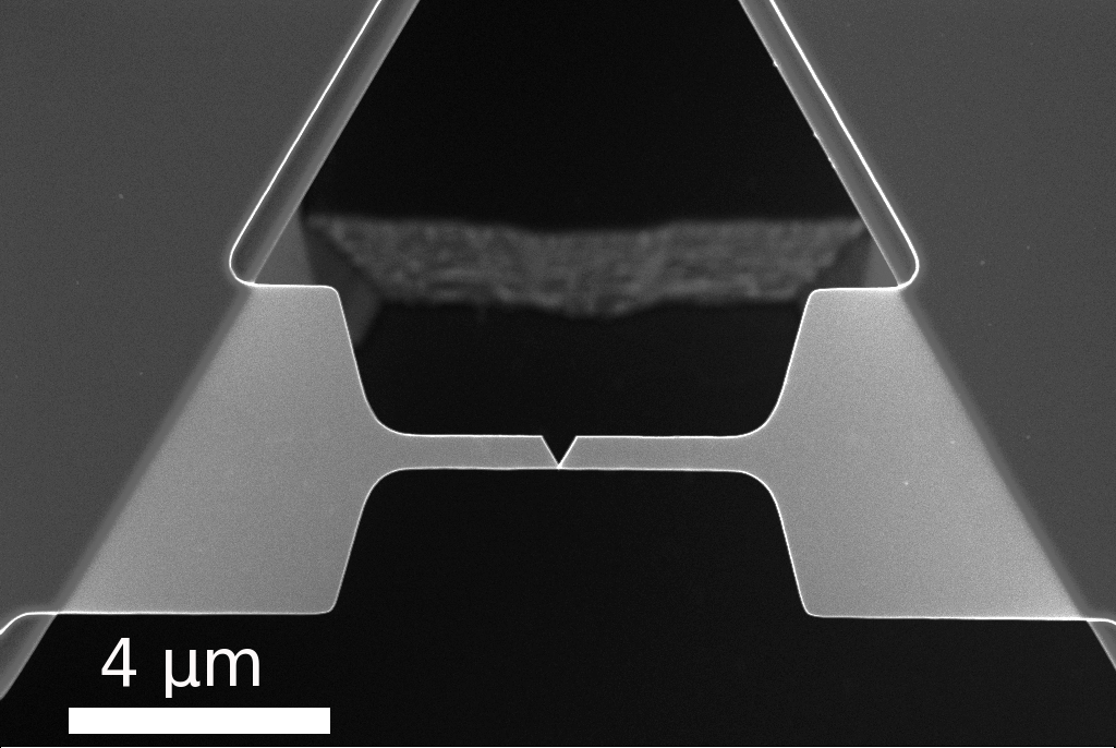
graph of a fractured nanobeam. The V shaped notch is not part of the fabricated design but a
characteristic of the failure mode.
We have developed a method of testing the fracture strength of doubly clamped beam specimens. The method uses a calibrated atomic force microscope to deform the specimen until fracture occurs. The focus of these experiments is the relationship of the surface mechanical and chemical condition to the measured strength distribution.
Sample Fabrication Process
The double clamped beam test specimens, such as that shown in the above
image, are fabricated using standard microfabrication techniques at the Cornell Nanoscale Science and Technology Facility (CNF) from (111) oriented Si wafers.
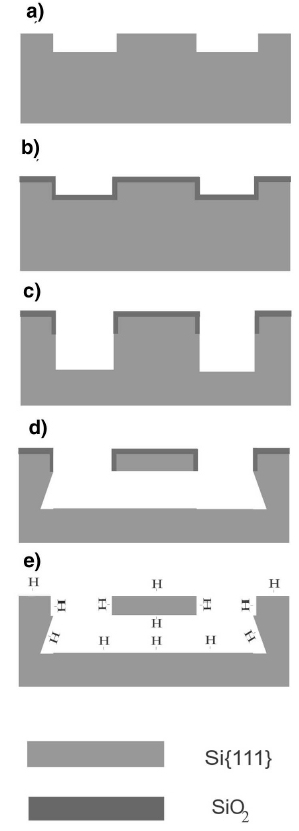
In part (a), the shape of the the beams are defined using photolithography. Reactive ion etching (RIE) is used to etch to a relatively shallow depth. The depth of this first etch controls the thickness of the final beam structures. A 100 nm thick thermal oxide is then grown over the etched surface, shown in part (b). Photolithography is used to generate a similar pattern and another round of RIE is done as is seen in part (c). At this point the bottom of the beam is still connected to the rest of the wafer by a pillar of Si. The beams are released by an anisotropic wet etch that removes all non-{111} surfaces in part (d). This etch is done using potassium hydroxide (KOH) and tetramethyl ammonium hydroxide (TMAH). Because the top and sides of the beam are protected by the thermal oxide and the bottom is a {111} termination plane the beam is now suspended across a trench. In part (e), the oxide layer is removed with a buffered oxide solution (5:1 NH4F:HF) leaving a clean, H terminated surface. If desired additional steps may be performed to functionalize this surface.
AFM Based Testing Method
The fracture strength of the beams is tested using an atomic force microscope (AFM) as shown below. For fracture strength testing, we position the cantilever tip at the center of the beam and force the beam to deflect until it breaks. During the test, both cantilever and beam deflection are recorded simultaneously. If the stiffness of the cantilever is known this can be used to produce a force-displacement curve for the beam. A finite element model of the beam is then
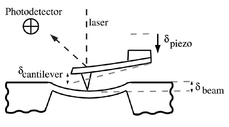
used to convert either the force and failure or the deflection at failure to a stress at failure. Like many brittle materials, Si fails in a stochastic manner, thus only by testing a number of beams in this way can a strength distribution be obtained.
Past Results
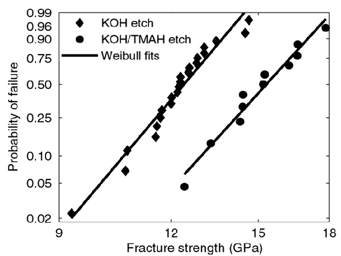
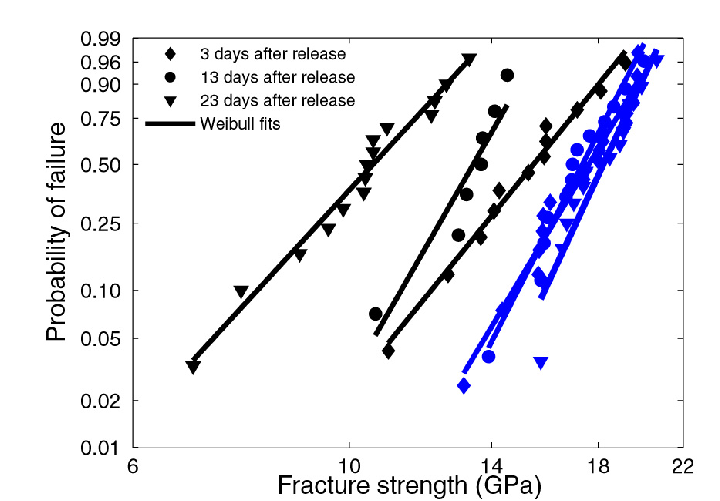
Using the fabrication and testing results described above our prior work showed that the strength of Si beams depends strongly on their surface properties. Specifically, they demonstrated that a smoother beam surface gives rise to stronger beams. This is shown in the plot below. The KOH etch produces a rougher surface than the KOH/TMAH etch and as a result is associated with lower strengths. They also demonstrated that beam strength decreases with time since release, presumably due to the development of a native oxide layer on the surface. This hypothesis was supported by the fact that if an organic monolayer which inhibited surface oxidation was used the initially high strength was maintained. In the plot on the right below the black lines are where the native oxide was allowed to develop and the blue lines indicate the use of the organic surface treatment inhibiting oxidation.
New Results:
approximately one year.
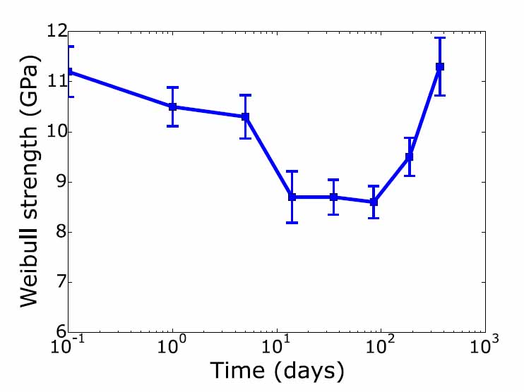
Results of the experiments show that over a period of roughly one month the strength of initially H terminated Si(111) surfaces decreases by about 25% with most of the change occurring in the first two weeks. This strength change can be shown to be a result of changes in the Si surface due to oxidation. By comparing the level of strength change to previous experiments that studied the effect of roughness on strength,3 and by observing that scanning tunneling microscopy studies show that a similar roughness results from oxidation of an initially flat Si (111) surface, we conclude that the strength change is a result of atomic scale roughness caused by oxidation. Molecular dynamics simulations corroborate this by showing a decrease in strength with small surface steps that is similar in relative terms to the decrease associated with partial oxidation over time of up to 100 days.

Acknowledgements:
This work was supported by NSF grants CMMI-0856488, DGE-0654193 and DGE-0654193. It was performed in part at the Cornell NanoScale Facility, a member of the National Nanotechnology Infrastructure Network, which is supported by NSF Grant ECS-0335765, and made use of the X-ray diffraction and AFM facilities at the Cornell Center for Materials Research (CCMR) with support from the NSF Materials Research Science and Engineering Centers (MRSEC) program (DMR-1120296). We would also like to thank our collaborators in the Nanomechanical Properties Group at the National Institute of Standards and Technology in Gaithersburg, MD for their contributions.
Any opinions, findings, and conclusions or recommendations expressed in this material are those of the author(s) and do not necessarily reflect the views of the National Science Foundation. Specific commercial equipment, instruments, and materials that are identified in this report are listed in order to adequately describe the experimental procedure and are not intended to imply endorsement or recommendation by the National Institute of Standards and Technology.